Mark Hofmeister
Beethoven Clock
Client
Normal Industries, LLC
Location
Pittsburgh, PA
Year
2024 (In Progress)
Resources

While the design of Sinking Clock was wrapping up, Ross and I decided to collaborate on a second time sculpture - the Beethoven Clock. This is Ross's third time sculpture and the second digital one for which I've designed the electronics.
To save time and money, I was able to reuse many modules from the Sinking Clock project, which I'd check out first if you haven't already. However, this design differs greatly in the LED display requirements, form factor, and the requirement to play a high-quality audio clip.
Final Product Coming Soon!

System Requirements
I began work on this project with the mechanical enclosure & user interface almost entirely designed. I had to fit my tech package within pre-defined mechanical, electrical, and UI functionality constraints. My challenges were exacerbated by the goal to sell this product to international customers.
Specifically,
-
Tangible, Graphical, and Audial User Interface: The user must set display brightness, change the time, configure an alarm, and snooze the alarm in a preconfigured manner. The alarm sound must be a high-quality portion of Beethoven's Fifth Symphony.
-
Electronics Package: The PCBs must have a specific shape with exact mounting hole locations
-
International Power Constraints: The device must be able to be plugged into wall power independent of international location. This means that it must work with 120VAC and 240VAC wall power, as well as with different outlet configurations.
-
Uninterruptible Power Supply: If wall power is to fail, the clock timer must be able to remain functional, requiring the use of a backup battery.
-
Shipping: The device must be able to be shipped to most countries
-
Economical: The device must be as inexpensive as is realistic without sacrificing quality.
System design
My mistakes & lessons learned with Sinking Clock gave me insight into the system architecture, which is largely duplicated in this design.
However, this clock requires a quality audio clip rather than a simple buzzer. Therefore, I added a SPI flash memory chip on which to store an audio file. I'm loading the audio clip on the memory chip through an external programmer module, so I include a set of tri-state buffers that can be disabled to isolate the SPI bus from the MCU, which allows me to use the external programmer module without MCU SPI signal interference.

When the alarm goes off, the MCU loads audio data chunks from the flash memory chip and outputs them to a 3W amplifier over an I2S bus. The amplifier output is connected to a 4-ohm speaker. I also included a +5V rail to power the current-hungry amplifier and 7-segment displays to allow me to use a smaller +3.3V regulator and power rail.
Design Reuse
While the Beethoven Clock's exterior look and form factor are entirely different from Sinking Clock, the software and much of the hardware are duplicable. Only the colored portions of the below system diagram are new system components - the hardware/software for the rest are almost entirely reused. This saved me tremendous hardware design time, software writing time, and PCB revisions since I knew much would definitely work. Of course, saved time = saved money as well.

prototyping
I chose a 3W amplifier with a development board to allow me to determine hardware configuration before ordering Mk. I PCBs. I was able to jump the I2S signals from my STM32 Audio Dev panel PCB and immediately test the amplifier configurations.


While the SPI connections to the flash memory chip are straightforward, I decided to solder one to an adapter board and talk to it with a NUCLEO. This allowed me to write + test the C driver and test the DMA transfers to the amplifier while the PCBs were being manufactured. I wrote the libraries to be as "drag-n-drop"-friendly as possible.
Brain PCB - MK. I
The Mk. I PCB had to be 45mm x 105mm and has the below barrel socket, buttons, and speaker placement fixed by Ross. There could be no components other than the buttons + switch on the backside of the PCB, so I had to pack a lot of circuitry onto the top. Therefore, I had to do some minimization; for example, I replaced the large electrolytic capacitors (which I was using on the linear regulator inputs for their high ESR) with series MLCCs + 5-ohm 0402 resistors. As opposed to the Sinking Clock Brain PCB, the Beethoven Clock Brain PCB is 4 layers, as routing power + ground on 2 layers on this dense board would've been tough. I also wanted a dedicated reference plane for my SPI signals.

Front

Back
Everything in the system diagrams is contained in the Brain PCB, except for the shift registers and 7-segment displays, which are powered and communicated with through a JST SUR connector.
Unfortunately, I didn't have much of a choice with the capacitive touch electrode connector placement. The user touches an elliptical section on the front of the clock enclosure to silence the alarm, which is oriented such that the electrode will have to bend like so (viewed from the side.)


Since the barrel socket position was fixed, I had to place the screw terminal right in the middle of the board. This is not ideal for capacitive touch sensitivity, so I tried to minimize as much local parasitic capacitance as much as possible with polygon voiding.
As usual, I included assembly drawings to ensure crystal-clear communication with the manufacturer + assembler.
This includes silkscreen indicator clarifications and tidbits about what is acceptable.


I paid particular attention to the speaker assembly. I made a 3D model of the red + black wires protruding from the speaker to show exactly how they should be wound through the strain-relief holes and soldered into the through holes, as I don't want one of the wires coming loose during the mounting of the PCB inside of the enclosure.
This paid off - the PCBs arrived looking + working great. No mistakes have been detected to date.


LED pcb - MK. I
Unlike the Sinking Clock, the design uses small COTS 7-segment display modules, rather than a large display requiring custom LED segments. However, the 4 required digits are grouped into two groups of 2, each of which make up one of Beethoven's eyes. Therefore, each PCB is only 2 shift registers wide:

I wanted to reuse my shift register hardware/software to drive the displays, but Ross's assembly and size constraints are unique. Therefore, I designed tiny 19mm x 12mm PCBs to "backpack" the 7-segment display modules. I'm using the same shift registers as those in Sinking Clock but in a much smaller QFN package and ones to accept TTL logic levels (Since they're powered by 5V now, not 3.3V) to avoid level shifters. The shift registers can sink just enough current to drive the LEDs bright enough, which avoids driving external FETs, which wouldn't have fit on the boards anyway.
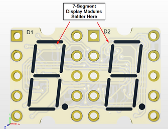
Front

Back
To fit everything on the PCB, I used JST SUR series 8-position connectors, which only have a 0.8mm pitch. These deliver 5V power and 5 signals to the shift registers, the outputs of which in turn act as sinks for the 7-segment display module LEDs. I designed the PCBs with both an input and output connector, allowing multiple LED PCBs to be wired in series and effectively serve as 4 series shift registers. That way, only one long 8-position cable need be run to the LED PCBs and my sinking clock shift register libraries can be reused.

My boards barely meet fabrication and assembly specs, but the first batch works great and I did it on 2 layers.
Flex PCB - Mk. I
I'm using the same connector and pad shape for this flex electrode. I continue to use 4 capacitive touch channels for redundancy, as I've had experiences with traces breaking and nullifying a channel on Sinking Clock Flex PCBs. However, the bend angle for this Flex PCB is much different and more extreme than that of Sinking Clock.

To avoid breaking the traces, I sensed a critical point where the exposed pads touching the screw terminal metal connect to the hatched traces/pads. Therefore, I added a stiffener on the top side of the PCB to create mechanical integrity by this critical point. Unfortunately, I don't have exposed copper pads on the top and bottom sides of the PCB to contact the screw terminals, but this is a trade-off that I'm willing to make.

Firmware
Below is a gallery of the file structure, main thread, and interrupt callback functions from the RTC and user buttons. I've abstracted out some error-checking and trivial operations, which can be investigated in the source code (if desired.)


The audio clip is almost 2 minutes long and needs to be reasonably high fidelity across the entire spectrum. Though I have one speaker, I2S requires stereo audio input.
I could compress the audio into a file format like .mp3 to minimize the size of the flash memory chip. I'm not using a terribly fast or powerful MCU, so uncompressing this data would require a more powerful MCU or an external chip, the additional costs of which would far overshadow those saved by using a smaller memory chip. Therefore, I'm sticking to an uncompressed WAV file.
A 2:00 stereo audio clip is 20MB, requiring a 32 MB flash memory chip (based on available memory sizes.) Stereo audio is unnecessary in this instance, so I store a mono audio file on the flash memory chip. This cuts the audio file size to 10MB, only requiring a (much cheaper) 16MB flash memory chip. The I2S amplifier requires a stereo audio stream, but I have enough processor resources to interleave zeroes in between data chunks and can tell my amplifier to pay attention to only the channel with the non-zero data.
The SPI interface only receives 8 bits of data per RX cycle, but the I2S interface requires 16-bit samples. Therefore, I'm using the CPU to concatenate 8-bit chunks into 16-bit samples and insert zero half-words after every data half-word. To provide a constant stream of audio and offload data transfers from the CPU so it has enough time to process data, I'm using two DMA streams to double-buffer data transfer. One stream ping-pongs between filling two buffers with new data from the SPI interface and another continuously loops through pushing processed data from another buffer to the I2S interface:

Production Run
A few trivial changes were made to the designs (silkscreen font, etc.) and production runs of 25 units were ordered. I also fixed a few trivial software bugs.
Mk. I of the LED PCBs and Flex PCBs were perfect. I only REVed the Brain PCB to Mk. II because Ross decided to elongate the PCB dimensions and change the font.


All PCBs had a 100% yield rate, even the 50x LED PCBs with very tight clearances.